The Advanced Semiconductor Packaging Technology workshop is designed to provide in-depth knowledge and practical insights into modern semiconductor packaging techniques. As the demand for high-performance, compact, and energy-efficient electronic systems continues to grow, advanced packaging plays a critical role in enabling next-generation innovations.
This workshop brings together industry experts, researchers, and professionals to explore cutting-edge technologies such as 2.5D/3D integration, System-in-Package (SiP), and wafer-level packaging. Participants will gain a comprehensive understanding of design, materials, manufacturing processes, and reliability aspects of semiconductor packaging.
Through a combination of expert sessions, case studies, and interactive discussions, attendees will be equipped with the skills and knowledge needed to stay ahead in the rapidly evolving semiconductor industry.
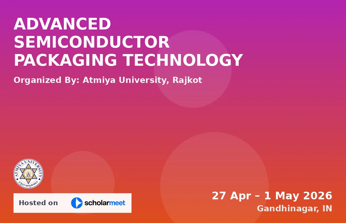
GUJCOST Sponsored Five Days Workshop on ADVANCED SEMICONDUCTOR PACKAGING TECHNOLOGY
E-mail: hiren.bhatt@atmiyauni.ac.in | Mo. +91 9879349424